Electromagnetic Compliance: Troubleshooting with Near-Field and Current Probes
October 20, 2017
Electromagnetic interference (EMI) can cause a host of problems, especially when developing a product or attempting to pass mandatory electromagnetic compliance (EMC) tests. Garbled displays, bad data, or complete malfunctions can occur when a design is effected by EMI. To minimize the effects of interference, government agencies like the Federal Communications Commission (FCC) in North America create and enforce standards that set limits on the EM output of a product type. Testing to the specifications is commonly referred to as Electromagnetic Compliance (EMC) testing.
Many EMC test failures stem from the interaction of unintentional radio frequency (RF) emissions with a circuit or element within the design itself. The electric and magnetic fields that cause this interference are not visible to the unaided eye, which can present complications when trying to isolate the root cause and minimize the effects of the EMI.
- What is causing the issue?
- Where is the source of the signal or energy causing the radiation?
- How can I fix it?
Fortunately, there are simple tools and techniques that can help identify the sources of EMI. Once you can identify the source, you can begin to build up a list of solutions to the problems. These techniques are not part of the mandatory compliance tests required to pass EMC testing. Rather, these are pre-compliance test techniques that help identify potential areas of EMI as quickly as possible without the burden of expensive test equipment and setups.
In this application note, we are going to introduce some common pre-compliance test techniques for identifying potential problematic EMI sources using near-field and current probes. These techniques can save you time and money by isolating problem areas quickly, and with a little fixturing, you can create repeatable test stations to help correlate data. This knowledge can then be used to “design for EMC” in your future products.
NOTE: Pre-compliance tests are designed to help identify and resolve issues that may hinder passing full compliance tests. Pre-compliance testing is not a replacement for full compliance testing at a certified lab.
ELECTROMAGNETIC RADIATION BASICS
In electronics, EM radiation is most commonly caused by a current flow or voltage buildup along or through a conductor. This includes traces on a PC board, discrete wires, component leads/pins, connectors, or any other metal, including the chassis, rack, or product enclosure. Recall that EM radiation is actually a combination of electric and magnetic field components. It is described as the propagation of orthogonal time-varying electric and magnetic fields as shown in figure 1.

Figure 1: Electromagnetic wave propagation out of the page (top left), to the right (top right) and out of the page at an angle. Note that the E and H fields are orthogonal (90°) to one another.
While the electric (E) and magnetic (H) fields are created by the same phenomena, they physically behave quite differently in the environment. Magnetic fields are only created by moving charges (current). In most circuits, current is conducted by traces on the PC board, component pins/leas, and discrete wires. Therefore, the magnetic field tends to dominate the EM radiation produced by the traces and wires that route signals and power to different parts of the design.
Visualizing the magnetic field can be a bit easier if you go back to your Physics texts. Recall that the magnetic field of an infinitely long straight wire can be calculated by applying Ampere’s law:

For a circular path centered on the wire, the summation becomes:

Where:

Figure 2 is a physical representation of this relationship. Note, this is also described by the “right-hand-rule” wherein if you were to point the thumb of your right hand in the direction of the current flow, then the magnetic field lines form concentric rings that wrap around the conductor in the direction of your fingers.
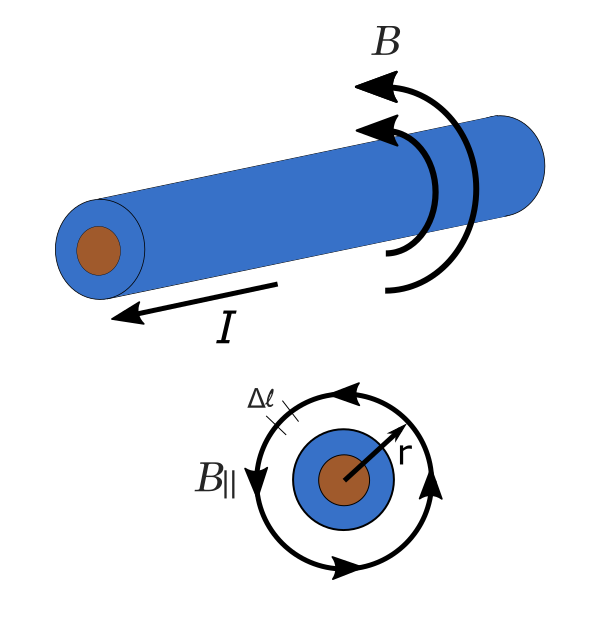
Figure 2: Magnetic field produced by a current
Unlike the magnetic field, electric fields can be created by moving or static charges. In this way, electric field effects dominate over magnetic fields when searching for EM radiation on surfaces like heatsinks or metal enclosures. The effects of the electric field also tend to dominate further away from the source (far-field). Far-field measurements are more susceptible to error due to environmental factors like radio stations, WiFi, and intentional RF. Far-field measurements, like those performed during radiated emissions portion of a compliance test, require more setup, equipment, and expertise than near-field.
By measuring the amplitude and frequency of the magnetic and electric fields that are generated by elements of a product, we can identify the areas that have the highest potential to cause EMI issues.
EQUIPMENT LIST
Here are the basic requirements for a near-field troubleshooting kit:
Spectrum Analyzer/EMI Receiver: Measures RF power with respect to frequency. The analyzer should have a maximum frequency of at least 1 GHz, DANL of -100 dBm (-40 dBuV) or less, and a minimum RBW of at least 10 kHz.
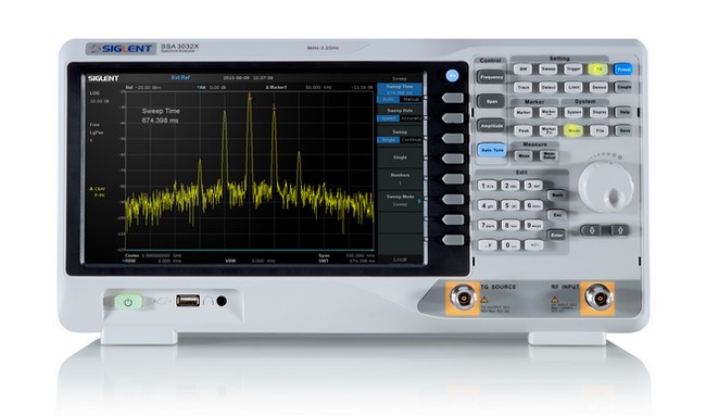
Figure 3: A SIGLENT SSA3021X 2.1 GHz spectrum analyzer.
Near-field probes: Commercial or handmade. Many are magnetic (H) field probes, but there are also electric (E) field probes as well.
Current probes: Commercial or handmade.
50 Ohm cable: Use a cable with connectors that mate to the near-field probes and the RF input of the spectrum analyzer. Many commercial probes can be purchased with a cable and any adapters that may be required.
PROBES
Since EMI cannot directly observed by the human eye, we need some tools to help. Recall that moving charges in a conductor produce magnetic and electric fields that radiate throughout space from the conductor. We can use these fields to induce a voltage in a circuit. Then, measure that induced voltage and therefore indirectly measuring the strength of the original field. The two most common types of probes used in EMI troubleshooting are near-field probes and current clamps.
Magnetic field probes and current clamps operate on a similar principle. The magnetic field that flows through the “loop” area of the probe induces a voltage that can be measured (figure 4). Larger loop areas pick up more magnetic flux, and are therefore better suited to finding smaller signals, but smaller loops offer better spatial resolution. Many kits come with multiple loop sizes (figure 5) to help strike the balance between sensitivity and spatial resolution.
Electric field probes do not generally have a loop area. They pick up the electric field similar to a monopole antenna. The rotation of an electric field probe is not critical as with the magnetic field probe, but the distance from the signal source is.
Here are some guidelines for probing:
- Measure the background radiation by powering off the device-under-test and monitor the analyzer display. Note any RF that may be caused by background or environmental conditions and retest often.
- Probe displays, communications port terminals, and any cutout/air vent/seam of the enclosure. These are common problem areas.
- E and H field probes positioned closer to the signal source will measure higher amplitudes
- H field probes oriented perpendicular to the magnetic field will measure higher amplitudes than those oriented parallel to the magnetic field.
- Since probe positioning is critical to repeatable measurements, a non-conductive fixture (wood, plastic) to position the device-under-test (DUT) and the probe can be used. Remember, position and orientation are very important. A few millimeters or a few degrees of rotation can cause a big difference in the measured amplitude of a given magnetic field.
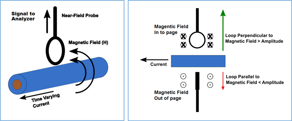 Figure 4: Magnetic field probe orientation and position affect measurement amplitude.
 Figure 5: SIGLENT SRF5030 near-field probe kit.
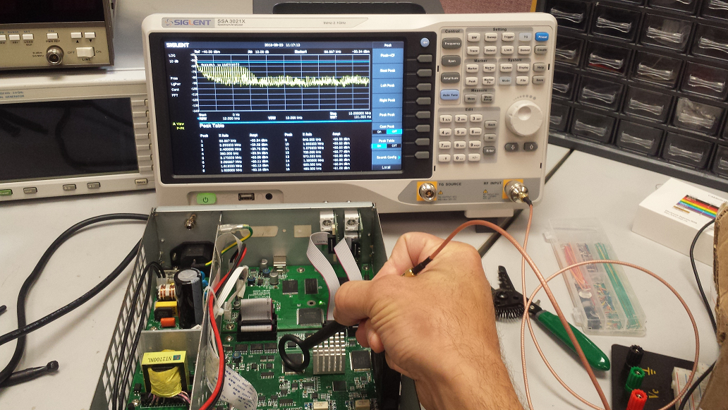 Figure 6: Probing a PCB using a SIGLENT SSA3X and SRF5030 probe.
Cables and interconnects can make very effective (and unintentional) antennas if they are not shielded/grounded correctly. Small currents flowing on the outside of the conductor can easily cause radiated emissions that can exceed the set EMC limits. A current clamp can be used with a spectrum analyzer to provide insight into the cause of radiating cables/interconnects.
Current clamps operate on the same principle as magnetic loop probes. They can be purchased or made by wrapping a few rounds of wire around a ferrite clamp and epoxy a BNC connector as shown in figure 7. Simply attach the clamp to the cable to be tested, connect it to the spectrum analyzer input, and configure the analyzer for the frequency span of interest.
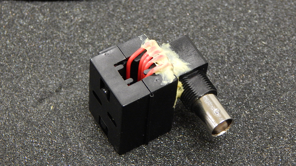
Figure 7: A handmade current clamp.
Here are some guidelines for probing:
- If in doubt, add an external attenuator to the RF input of the analyzer before you start. Power cables or expected high-power applications can have signals that will damage the sensitive RF input of the analyzer.
- Test all of the cables that could be connected to the DUT. This includes the power cord, USB, Ethernet, and any other possible connections (figure 8)
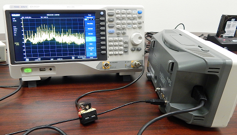
Figure 8: Measuring the RFI of a USB cable connected to a scope.
- Current clamps, especially handmade, are susceptible to picking up environmental RF that can skew or overwhelm the signals that you wish to measure. Connect and arrange all cables, probes, etc.. and then measure the environmental RF by simply keeping the DUT powered OFF. Then, compare it to measurements made with the DUT ON. It may also be a good idea to retest periodically to account for any environmental changes.
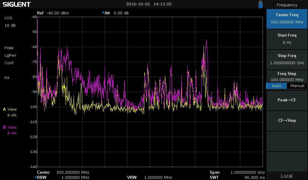
Figure 9: Traces of the environmental pickup from a current clamp (Yellow) and with the DUT powered ON (Pink).
- If you have a failed radiated emissions report, start by looking for the failed frequencies or for the first few harmonics of those frequencies.
SCANS AND EVALUATION
It is highly unlikely that data collected during probing will directly correlate to radiated emissions test performance. But, by observing the RF output of cables, switching power supplies, displays, and cutouts, you can have information that can lead to faster troubleshooting if you do happed to fail.
Here are optional techniques that can help provide more insight:
1. Most spectrum analyzers do not have pre-selection filters. If you are using a spectrum analyzer without pre-selection filters, the peaks you observe may not be real. Analyzers without pre-selection filters can create false peaks due to out-of-band signals mixing with the observed signals.
You can test the validity of a peak by adding an external attenuator (3 or 10dB should do). Real peaks will fall by the amount of the attenuator. If the peak falls by more than the attenuator, it is likely to be a false peak. Make a note of the false peaks for comparison with your compliance test results. You can also use pre-selection filters or an EMI receiver, but these tend to be cost prohibitive for most quick testing.
Figure 10 below shows a typical peak confirmation test. The yellow trace was collected without an attenuator. The Pink trace was collected with a 10 dB attenuator added to the RF input of the analyzer. In this case, the peaks drop the same amount as the added attenuation. This helps affirm that the peaks are likely real and not products of out-of-band signals.

Figure 10: Comparison of two scans using the marker table function of the SIGLENT SSA3000X spectrum analyzer. The Yellow trace was collected without attenuation while the Pink trace was collected after adding a 10 dB external attenuator.
2. Many spectrum analyzers have Max Hold trace types that will continuously hold the highest amplitudes of each frequency scan. You can enable a single trace as Clear Write to show active RF performance and enable a second trace as Max Hold. This allows you to compare changes in the DUT to the “worst case” data collected and “frozen” using Max Hold.
3. You can use markers and peak tables to clearly indicate peak frequencies and amplitudes, if available.
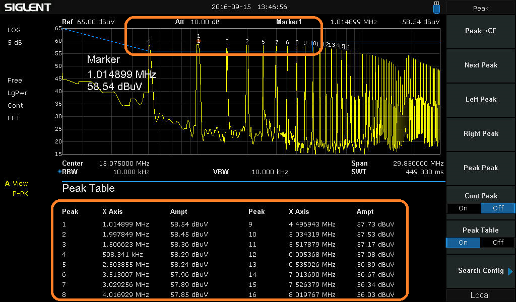
Figure 11: SSA3000X analyzer with Peak table and markers activated.
CONCLUSION
- Magnetic fields are produced by current flow. Use a magnetic (H) near-field probe to identify EM radiation near traces, wires, and ribbon/flex cables.
- Electric fields can be produced by current flow or static charge build up. Use an electric (E) near-field probe to identify EM radiation on metal surfaces like heat-sinks, enclosures, display bonding/edges, and slots/cutouts.
- Use current clamps to identify potential radiation and resonance from cables, wires, and interconnects
- Displays, cutouts/holes/seams in the chassis, ribbon cables, and communications ports/busses are the most likely cause of radiated emission failures.
- Use conductive tape or aluminum foil to cover areas of “leakage”, making sure that the covering is grounded. Rescan with the tape/foil in place to see if it has mitigated the EMI.
- Poorly terminated cables and interconnects also cause radiated issues
- Frequently measure the background effects by removing power from the device-under-test and monitor the output on an analyzer. Note any changes and their potential effects on the measurements.
With a few simple tools, you can implement an in-house pre-compliance test process that will minimize the total development time for your products, lower the cost of design, and decrease the amount of testing on future products.
For more information, check the SSA3000X webpage, or contact your local SIGLENT office.
