Power Supply Design: Load Step Response with a SIGLENT DC Electronic Load
April 3, 2020
Building a power supply that can handle various loads without oscillating can be a challenge. Computational models and computer simulations can help get your design headed in the right direction, but physical testing is essential to proving the performance of your design.
One method of quickly determining stability is to use a load step response.
In this test, a DC electronic load is used to provide a current load that steps from a low current draw to a higher value in a short period of time. By directly measuring the voltage and current output of the supply with the stepped load, we can visually observe the recovery of the power supply feedback loop and make changes to the design to optimize the response.
For this note, we are going to perform identical tests on two supplies and compare the output voltage and current waveforms: One has been tuned so that the output quickly recovers with minimal overshoot and ringing. The other supply is not tuned and subsequently oscillates. We will also discuss some measurement techniques to help get the right data as quickly as possible.
We also have a video to accompany this note:
Power Supply Design: Load Step Response with a SIGLENT DC Electronic Load
The Equipment:
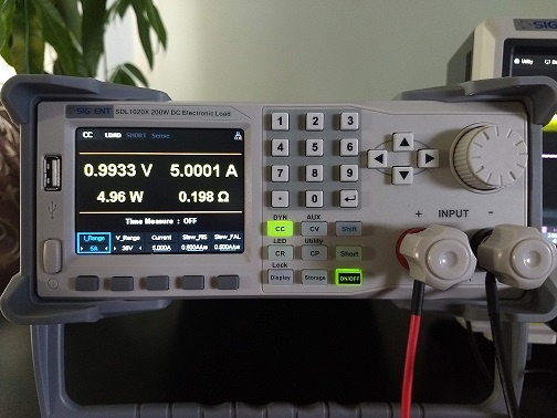
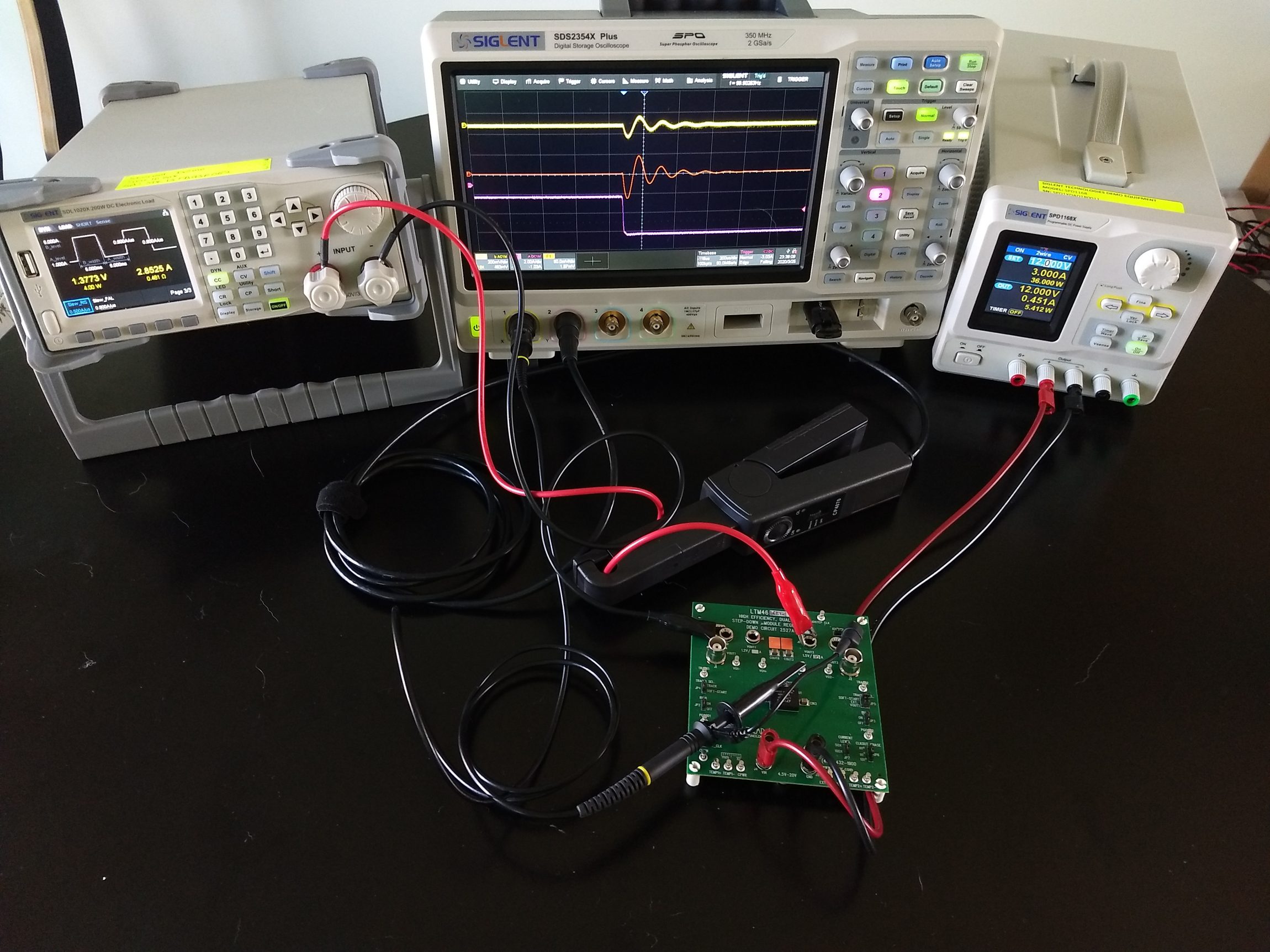
- A DC Electronic Load: The SIGLENT SDL1020X-E is a 200 W load with dynamic testing capabilities to perform the load step. It also features remote sense capabilities to compensate for the voltage drop across the load leads. High currents can provide a substantial voltage drop across the leads and will add unwanted error.
- An oscilloscope: The SIGLENT SDS2354X Plus scope has a large display, easy-to-use interface, and features that make capturing these waveforms very easy.
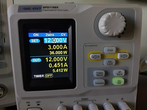
- A power supply: The SIGLENT SPD1168X single output supply delivers power to our power supply board
- A current probe: The SIGLENT CP4070 features a 150 kHz bandwidth that will minimize most switching noise from the measurement
- Power supplies to test: The Analog Devices LTM4646 series of uModule Regulators. This module features two 10A DC-DC converters. One has been “detuned” to show some common problems associated with power supply design. The other supply has been left in it’s tuned state as a comparison to the detuned supply.
The Setup:
- Connect the SPD bench power supply to the power supply to test and configure the output values to match your supply needs. Here, we set the SPD for 12 V @ 3 A.
- Connect the SDL electronic DC load to the output of the power supply to test. Configure the load for Constant Current (CC), set the voltage and current ranges to the lowest ranges that still accommodate the requirements of the test, set the current load to a value near the maximum for your design. You may also wish to wire up and enable the SDL remote sense which enables remote voltage measurement to minimize the voltage drop caused by the high current flow through the electronic load leads. Here, we set the current to 5 A.
- Connect a passive probe to the oscilloscope CH1. This probe should be connected to the power supply feedback loop to monitor the voltage as the supply adjusts to the load.
- On the oscilloscope, configure CH1 for AC coupling to provide the most resolution to view the feedback voltage which can have high DC offsets. Enabling the Bandwidth Limit (BW limit) can also decrease noise. Here, the SDS2X Plus also has on-screen labels for traces, which can be a convenient way of keeping information organized. Here, I labeled CH1 Vout.
- Connect the current probe to the oscilloscope CH2.
- On the oscilloscope, set the trigger for Rising Edge, CH2 and AUTO. This will allow you to adjust the current probe zero position without dealing with the trigger setting.
- Configure CH2 as a current probe (Units = A), set the Probe attenuation to the proper value (50 mV/A in this case). DC coupling here because we want to see the total signal amplitude. I also applied a label to the output current (Iout).
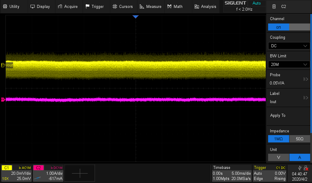
- Zero the current probe. The CPs have a knob that you can use to move the DC offset. Set the scope to a low current range and adjust the probe to get 0 A on the display.
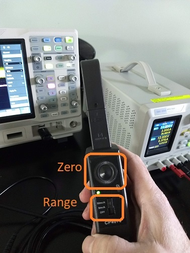
- Clip the current probe around the positive current lead going from the power supply under test to the DC load. Make sure to have the clamp connected such that positive current flow (into the load) produces a positive signal on the scope.
Now, everything is connected and ready to test:
Be on the lookout for interlopers and/or pesky critters wondering where the magic smoke came from:
DC Load Verification
Now, you can power on the SPD power supply and SDL load.
Make sure that the scope is set to AUTO trigger for now. You can also add an RMS measurement on CH2 so that you can verify the current draw matches the setting on the DC Load.
Here, we have a setting of 5 A on the DC load.. and we show 5 A RMS on the scope:
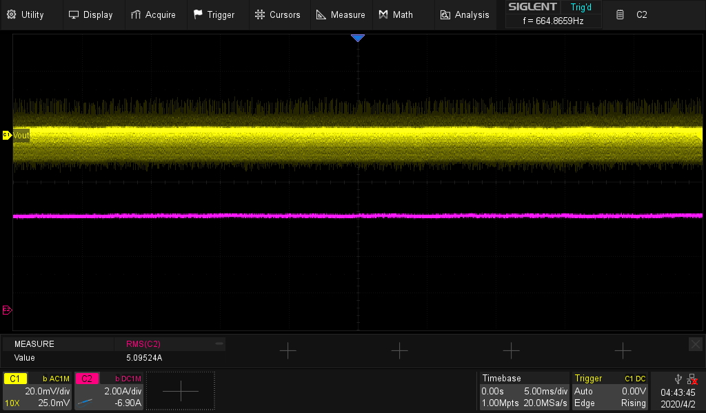
Things are looking good. The current output matches our load setting.
DC Load Step Response
Now, set the DC load to Dynamic Current mode by pressing Utility > CC.. and configure the appropriate ranges, low and high current values and duration, and slew rate for your application.
Here are the settings used for this test:
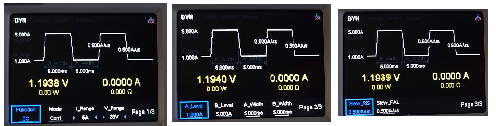
This will continuously cycle from 1 A for 5 ms to 5 A for 5 ms with 500 mA/us slew rate.
Now, switch the scope trigger mode to Normal and adjust the vertical, horizontal scales and positions.. as well as the trigger level to get a stable trigger and a few periods of transition on the display:
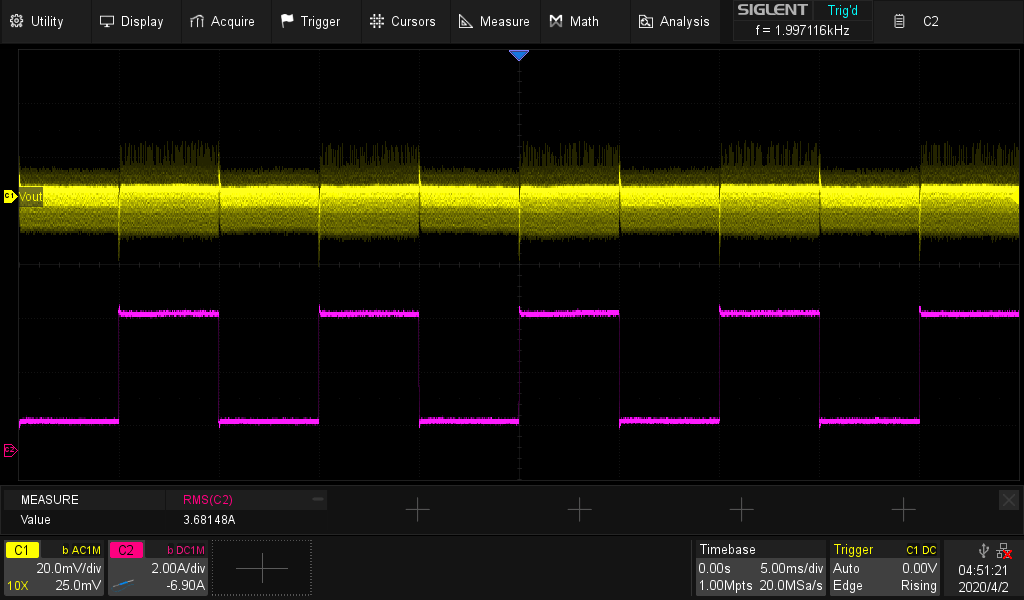
Verify that the supply high and low current values match the setpoints. For this example, we have 1 A for 5 ms and 5 A for 5 ms.. which is what we observe.
Observe and Optimize
Now, let’s compare a tuned setup to one that is not tuned for our load as well as some techniques to gather more information about the response.
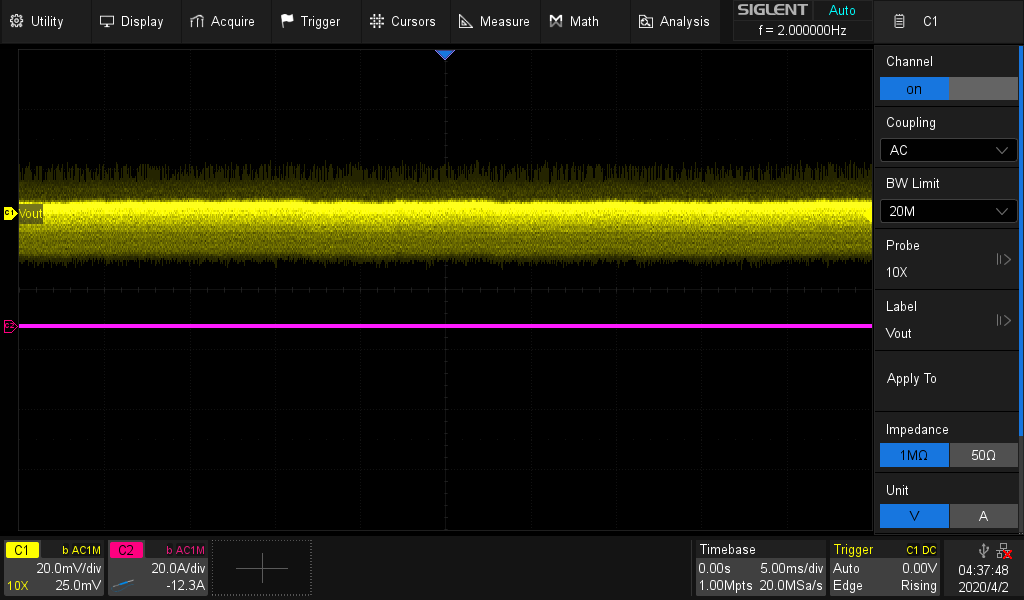
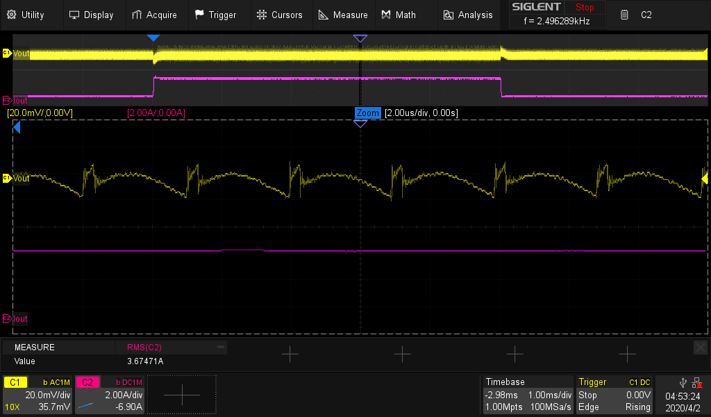
First, you likely see quite a bit of noise on your signal. The majority of this is due to switching noise in the supply being tested. Here is a zoomed image of the feedback voltage where you can see the switching noise quite clearly.
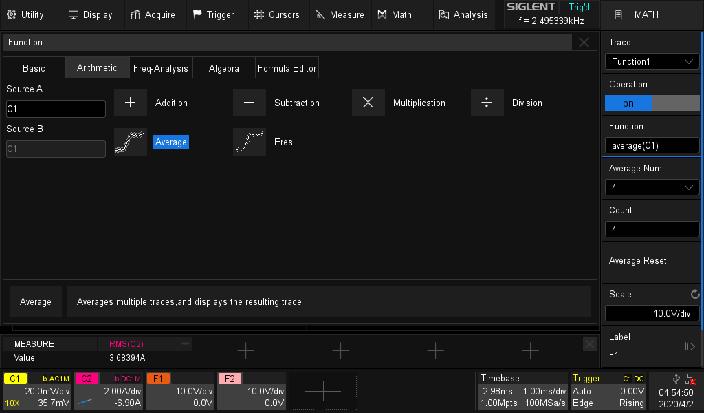
Enabling waveform averaging can help:
Now, we see the output voltage from CH1 (yellow), output current from CH2 (pink/purple), and the average voltage math function (orange):
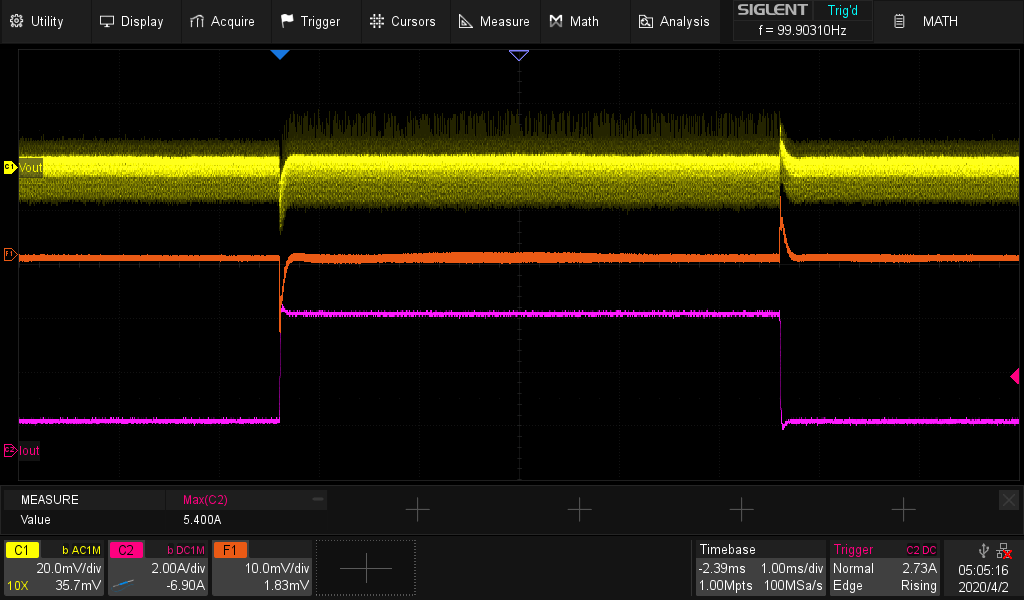
This is the tuned setup.
Now, let’s look at a detuned supply:
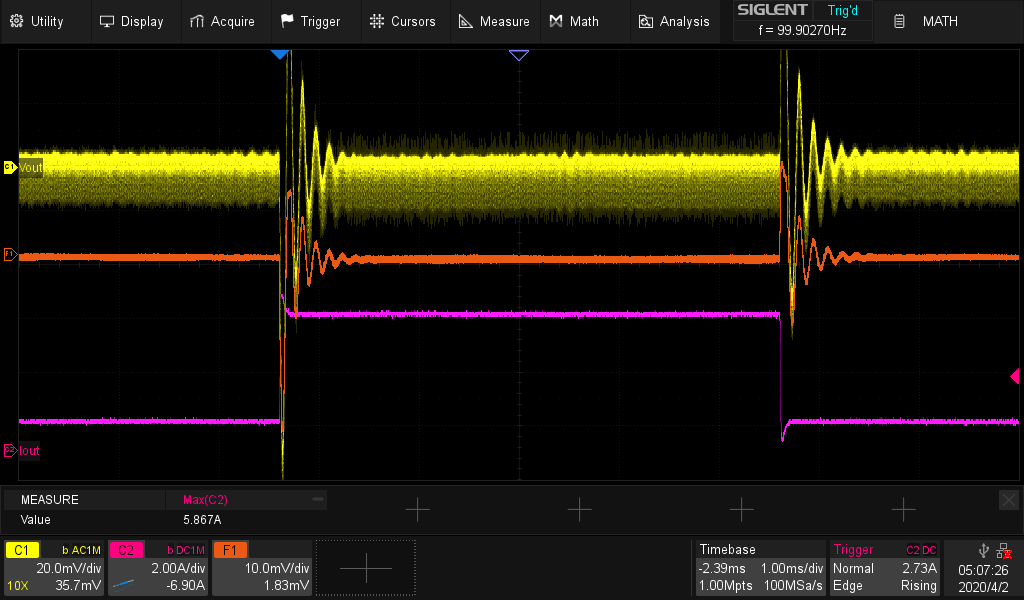
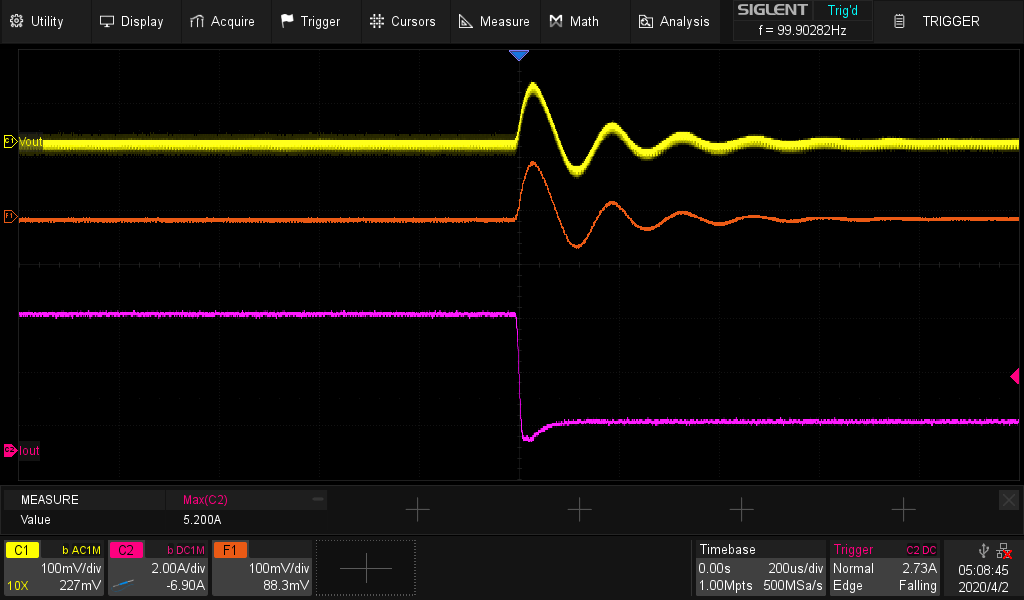
The scaling on these two images is exactly the same. You can see a large amount of ringing associated with the detuned supply. This design is very close to becoming an oscillator with this load. If our step duration was any shorter, the supply voltage wouldn’t be settled and our output would be very poorly regulated.
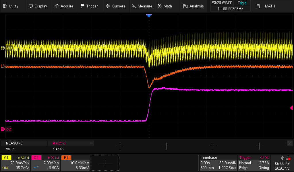
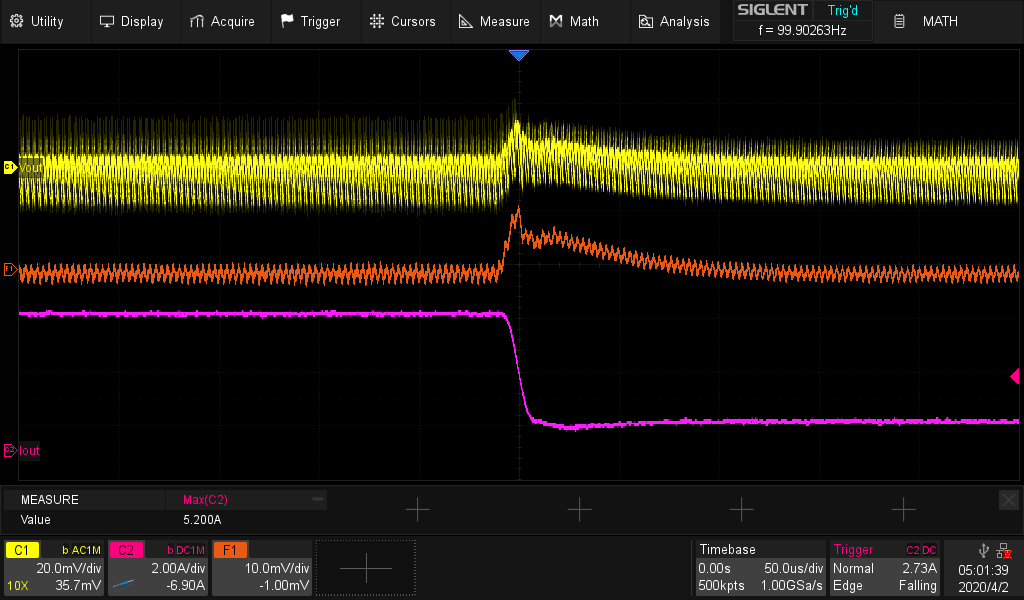
Here are some closer images of the rising and falling edges on shorter time scales:
Tuned, Rising:
Tuned, Falling:
Detuned, Rising:
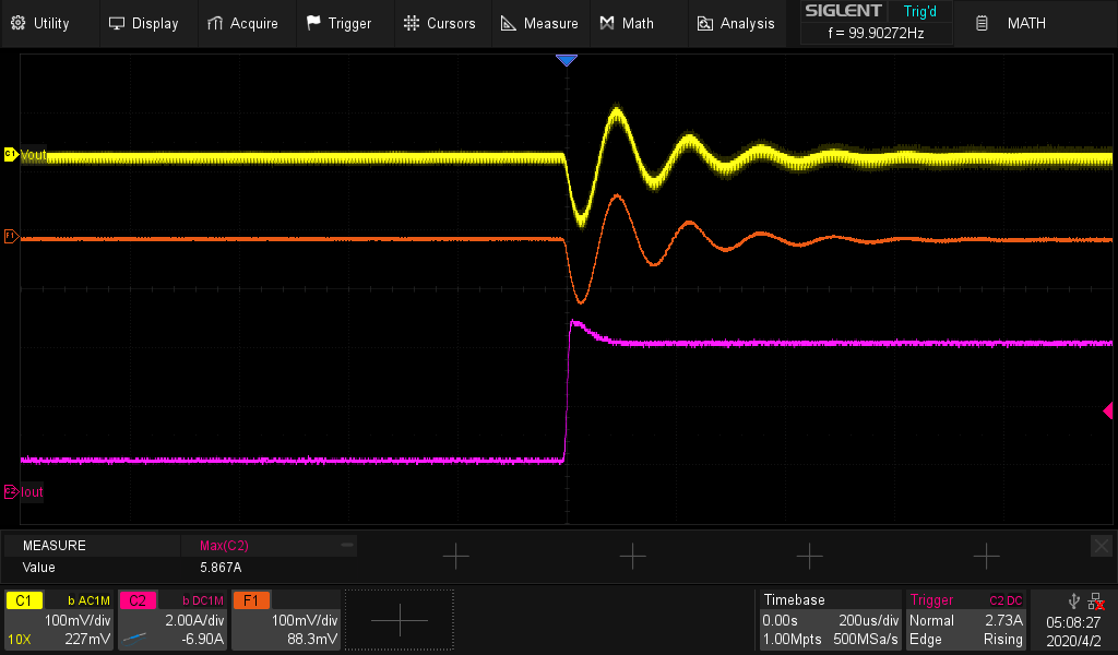
Detuned, Falling:
Conclusions
A DC load step test can quickly show you the performance and stability of a power supply design. Using a few common pieces of test gear, you can ensure that your design is ready to undertake the most challenging application requirements.